pcb - Connecting pads with the same functionality belonging to one
5 (549) In stock

I have a question about routing style of pads with the same functionality belonging to one chip. I draw a picture in Paint (fictional IC; let it be the SOIC8 footprint). GND is only as example (it

The complete guide to PCB pad :types, size, spacing, repair and comparison - IBE Electronics

An ultimate guide to PCB gold fingers - IBE Electronics

Types of PCB Pads PCB Knowledge - PCB Basic Information - PCBway
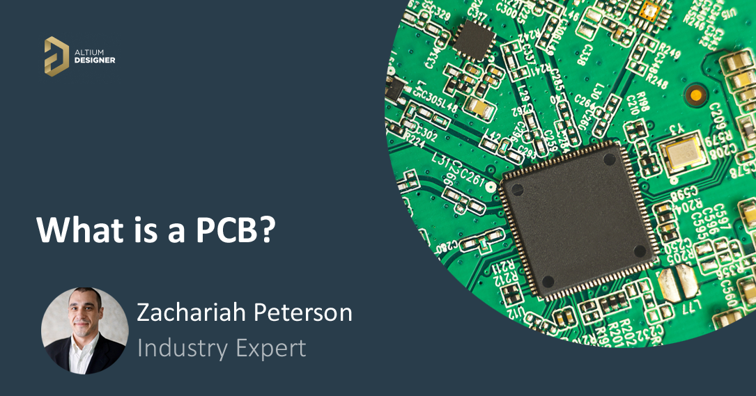
What is a PCB and PCB Design?
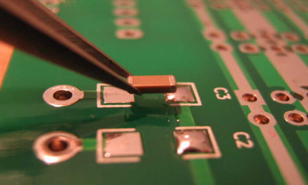
Fixing a Missing Solder Pad: What You Need and The Steps
PCB Basics knowledge
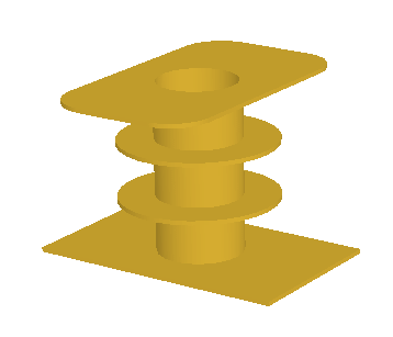
Working with Pads & Vias in Altium Designer Altium Designer 24 Technical Documentation
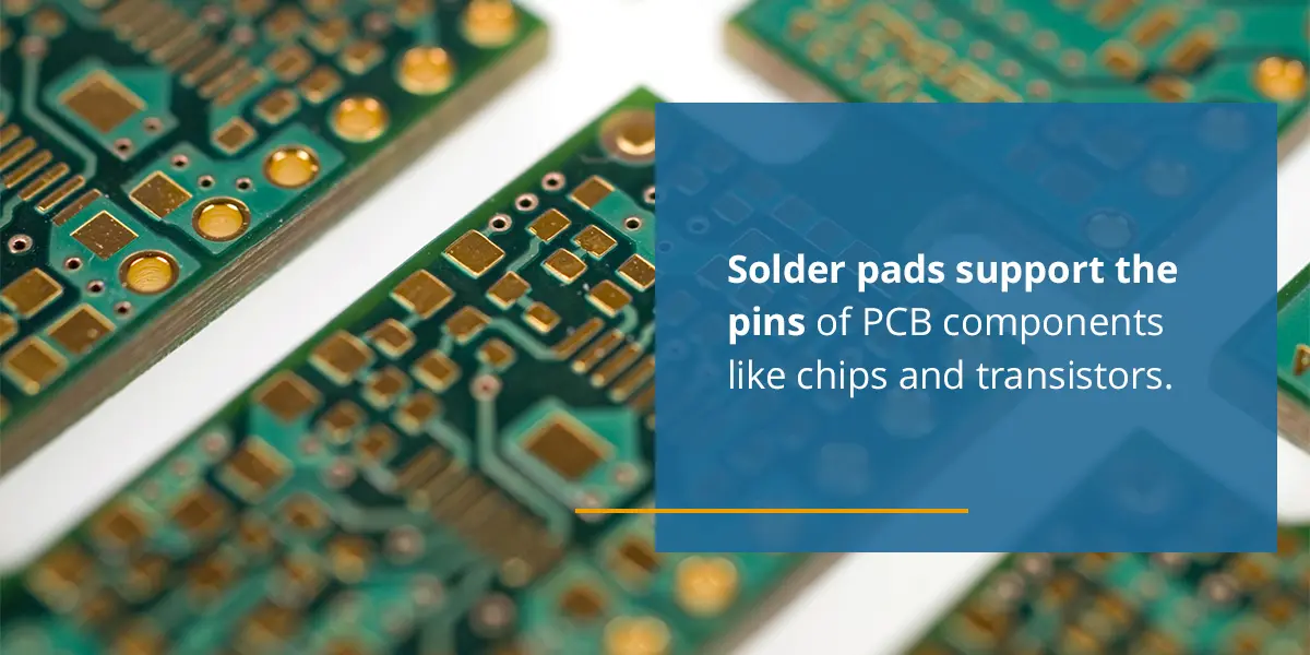
What Are PCB Pads? What Are Their Functions?
PCB Design Software - PADS
pcb design - A few questions about vias and pads on a PCB - Electrical Engineering Stack Exchange
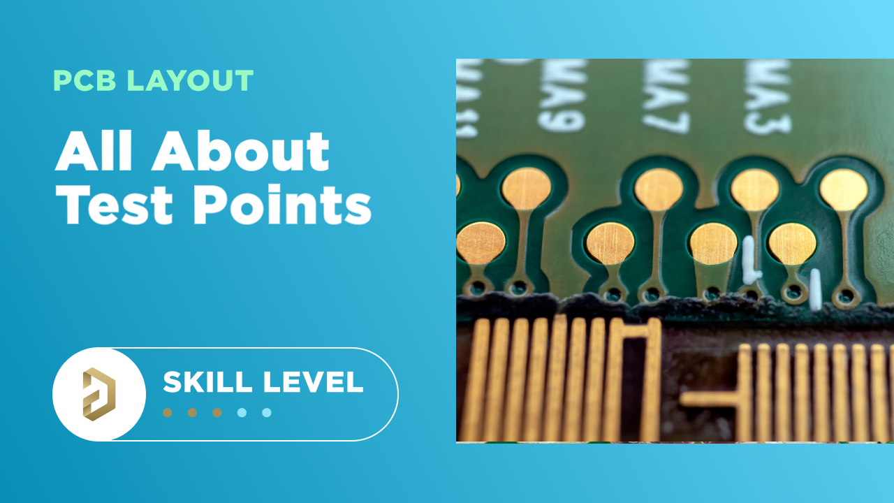
Is It Printed or a Component? All About PCB Test Points

What are PCB Pads? - RAYPCB
Guide to PCB Grounding Techniques
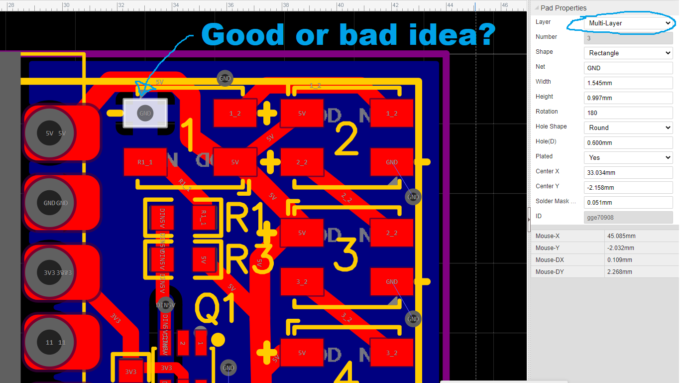
PCB Design, good or bad idea to use multilayer GND pads (to stitch plane and connect LED)? - Random or Off Topic - V1 Engineering Forum
Anion Chip Sanitary Napkin 240 mm at Rs 1.7/piece, Sanitary Napkins in Indore
12.9-inch iPad Pro Apple M2 chip - kite+key, Rutgers Tech Store
- Supima® Rib Halter Tank Top
 Dragons Cotton On Women's Icon Tights – Dragons Team Store
 Modest Women's Basic Layering Tank Top, Inherit Clothing Company
 Baby Panty Diaper Disposable Wholesale Training Pants Diaper - China Baby Pants Diaper and Diapers price
 Cream pop no steel ring thin shoulder comfortable seamless
 Supportive High-Impact Padded Convertible Sports Bra – PAVOI