The complete guide to PCB pad :types, size, spacing, repair and comparison - IBE Electronics
4.5 (611) In stock

Soldering is one of the most important processes in PCBA processing. On printed circuit boards, electrical connections to all components are made via PCB pads. The PCB pads are a very critical part of the PCB that determines where components are soldered on the PCB.The size, shape, and position of pads in a PCB directly depend on the manufacturing quality of the board. Today we will take a look at the PCB pad in SMT soldering.
Soldering is one of the most important processes in PCBA processing. On printed circuit boards, electrical connections to all components are made via PCB pad.
What are Vias in Pad? Advantages, Limitations, Applications, and Comparison with Conventional Vias
Solved Nep AutoZone Produces Brake Pads Using A Standard, 45% OFF

Xiaomi Packs 48-megapixel Camera Into Budget Redmi Note, 55% OFF
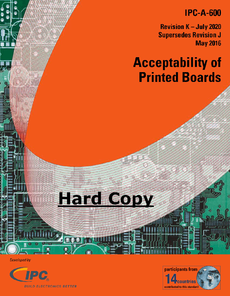
IPC-A-600: The Standard for Printed Circuit Board Inspection
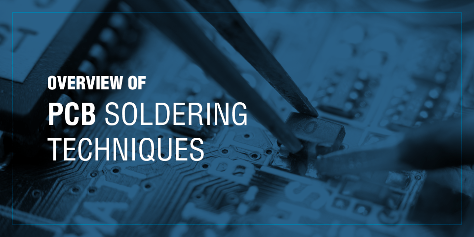
PCB Soldering Techniques What Soldering Equipment You Need

The complete guide to PCB pad :types, size, spacing, repair and comparison - IBE Electronics
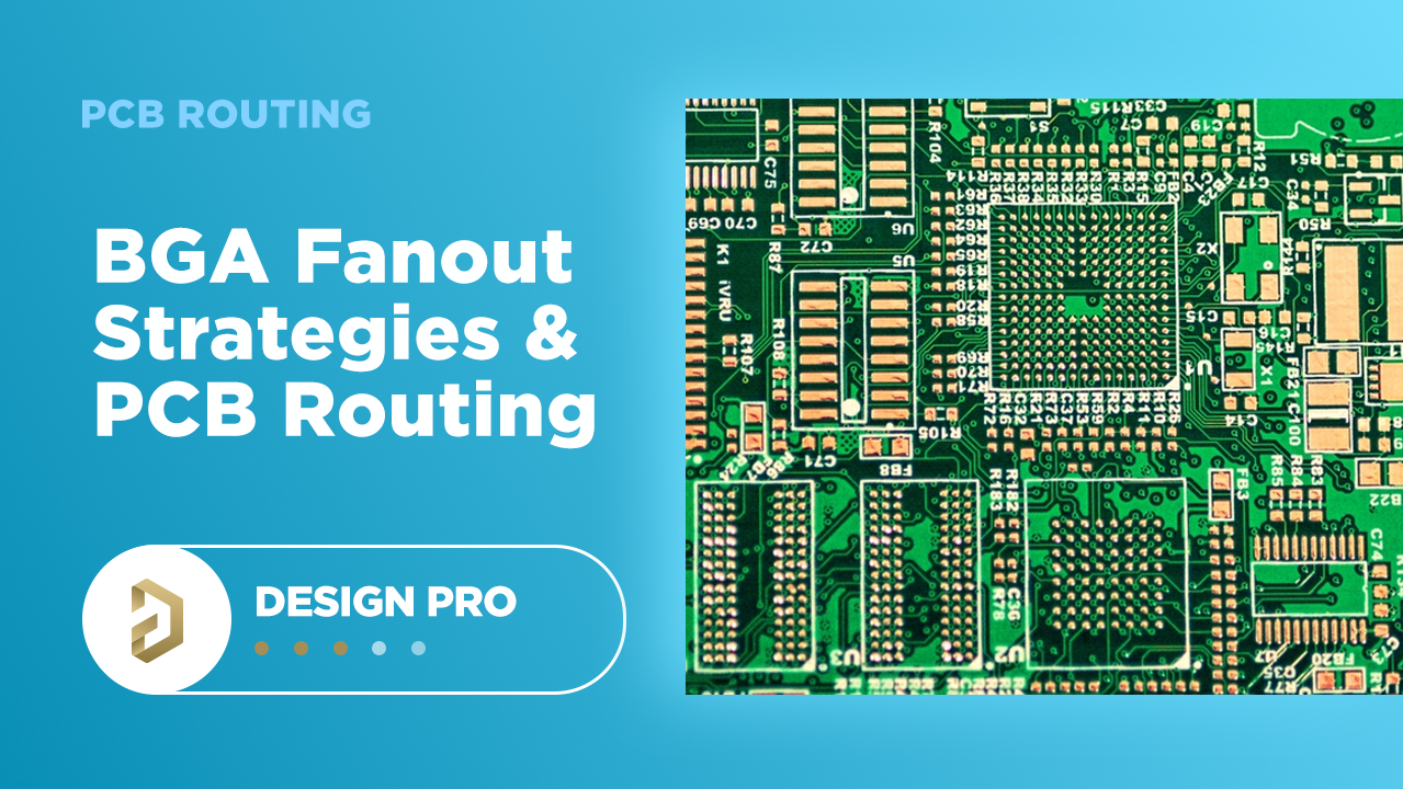
Which BGA Pad and Fanout Strategy is Right for Your PCB?
Trace Spacing: A Guide For PCB Design - Jhdpcb
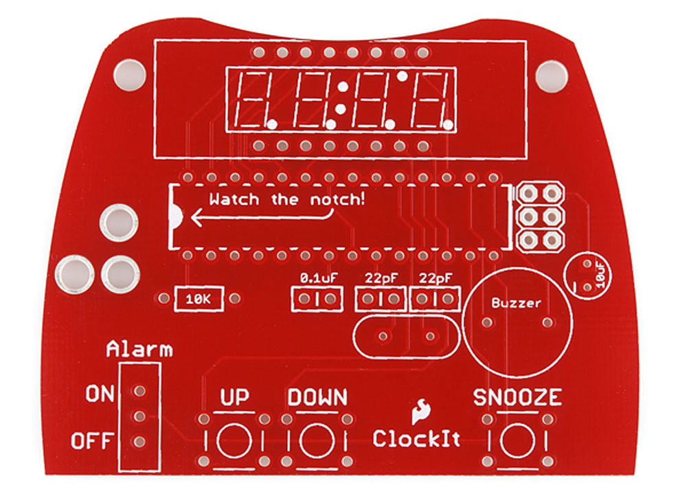
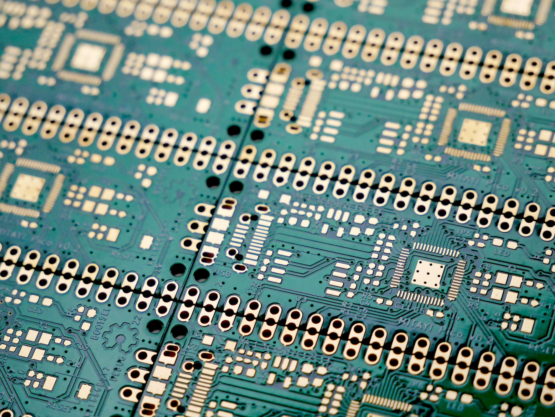
PCB Basics - SparkFun Learn
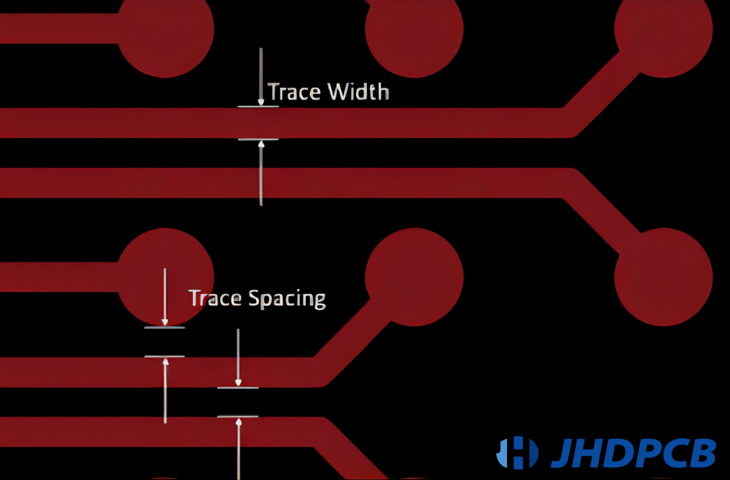
Trace Spacing: A Guide For PCB Design - Jhdpcb
Set fixed padding for components and groups
tensorflow - regarding the correct way to understand the result of
How Padding helps in CNN ?. An approach to build an efficient
Effect of sequence padding on the performance of deep learning
- Kydra Athletics - Ditch the rigid rules of minimum spending. This October, we are offering ⭐ FREE LOCAL SHIPPING ⭐on all orders (Applies automatically at checkout). What are you waiting for? Shop
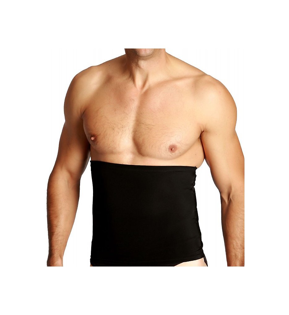
- Compression Slimming Belt by Insta Slim
 Smooth Duo Bike Short with Built-In Underwear 10
 Blusa Feminina Moda Pop Manga Curta Poa Bolinhas Decote Gota
 Pipe Fitting, Flare Elbow, Lead Free Brass, 1/2 Flare x 1/2 In. FPT
 Buy SPANX Brallelujah Mama Nursing Bra and Mama Short Online at desertcartSeychelles